Revolutionizing DIY PCB Fabrication: The Art of Soldermask and Silkscreen Application
In recent years, the landscape of circuit board fabrication has undergone a significant transformation. While low-cost professional printed circuit board (PCB) fabrication services have largely supplanted the once-common practice of crafting circuit boards at home, there remains an undeniable allure to the idea of designing and prototyping a custom board all in a single afternoon. Fortunately, today's technology has evolved beyond the traditional toner transfer method for DIY boards. Enthusiasts can now utilize CNC (Computer Numerical Control) routers and powerful laser systems to etch circuit boards with remarkable speed and precision.
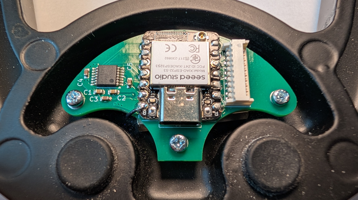
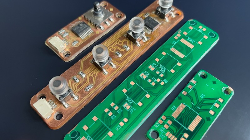
Despite these advanced methodologies, a persistent challenge remains: the boards produced by these techniques often feature exposed traces. While this might suffice for a quick, one-off project, such designs are inherently vulnerable to electrical shorts, compromising functionality and reliability. Additionally, aesthetically, they can leave much to be desired. This is where the innovation of maker and engineer Mikey Sklar comes into play; he has been diligently experimenting with the application of both soldermask and silkscreen to enhance the quality and appearance of his homemade circuit boards.
Sklarâs process begins post-etching, where he first applies a soldermask, a protective layer that prevents oxidation and protects the copper traces. Following this application, he sandwiches the board between layers of transparency film and clear acrylic, which is then cured under a UV light. This curing process solidifies the soldermask, creating a robust barrier against environmental factors. After two applications of soldermask, the board is ready for the next stage: silkscreening. Using a fiber laser, Sklar uploads the necessary silkscreen and mask layers into the machineâs software. A crucial aspect of this step is the adjustment of the laser's power settings; in this case, it is set to a relatively low 40%. Notably, the mask layer is programmed to run four times, compared to a single run for the silkscreen, which ensures that the underlying copper is fully exposed and highlighted.
One of the standout advantages of this method is that the board remains stationary throughout the entire process, eliminating the common issue of misalignment that can occur when transferring boards between operations. The end result is visually striking; the silkscreen component, in particular, stands out more vibrantly than one might initially expect.
This latest development is a natural progression from Sklar's previous work, where he utilized his CNC router and fiber laser to cut and etch PCBs. Now, the entire processâfrom design to final productâhas come full circle, showcasing an exciting and practical approach for DIY enthusiasts. While the equipment required to replicate this process at home may not be inexpensive, the impressive outcomes certainly validate the investment and effort involved in creating high-quality circuit boards.